Technical Notes
Filter by:
Product Category
20
9
4
3
2
2
2
1
1
1
1
Technical Notes
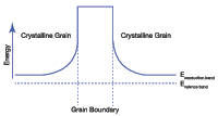
Polycrystalline Silicon Thin Films
Polysilicon thin films are produced using a process known as chemical vapor deposition or CVD. Heavily doped polysilicon and poly-silicide films have been used as gate electrodes and …
Technical Notes
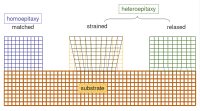
Silicon Based Epitaxial Thin Films
Epitaxy is defined as the "regularly oriented growth of one crystalline substance on another". Both homoepitaxy and heteroepitaxy processes are used in semiconductor device fabrica …
Technical Notes
Compound Semiconductor Epitaxial Thin Films
Compound semiconductors are materials such as GaAs, AlGaAs, GaN, CdSe, InP, InSb, etc. These materials combine the elements from equidistant columns on either side of Column IVA of …
Technical Notes
Dielectric Thin Films
Thermal SiO2 films for device components can be formed in a variety of ways; the selection of method is dependent on such factors as substrate composition/topography and the thermal …
Technical Notes
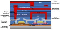
Metal Thin Films for Contacts and Interconnects
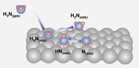
In semiconductor device fabrication, contacts are the metal components in direct contact with silicon in transistors and other devices, while interconnects are the current-carrying …
Technical Notes
Vacuum Pressure Basics
In simple terms, vacuum may be defined as: A space or container from which the air has been completely or partially removed.
Technical Notes
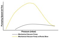
Creating a Vacuum
An in-depth understanding of the creation of vacuum requires consideration for physical characteristics such as gas viscosity, flow type, the thermal conductivity of the gas, and gas …
Technical Notes
Vacuum Measurement Principles
The first true pressure measurement was made by Evangelista Torricelli in the 17th Century, when he invented the mercury barometer and measured atmospheric pressure.
Technical Notes
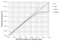
Pirani Thermal Conductivity Vacuum Gauge Physics
The Pirani gauge's sensing element is a wire of known resistance and known temperature coefficient of resistance.
Technical Notes
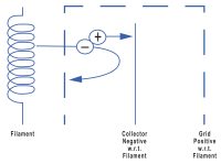
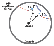
Ionization Vacuum Gauge Physics
UHV and XHV pressure measurements are routinely performed using ionization gauges configured as either hot cathode gauges (HCGs) or cold cathode gauges (CCGs).
Technical Notes
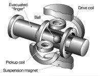
Spinning Rotor Vacuum Gauge Physics
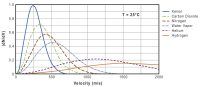
Spinning rotor gauges (SRGs) also known as molecular drag or viscosity gauges, measure the number density of the surrounding gas.
Technical Notes
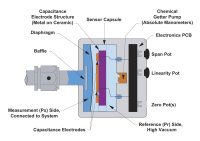
Capacitance Manometer Physics
The capacitance gauge translates a pressure-modulated movement in a thin diaphragm into an electrical signal proportional to the pressure.
Technical Notes
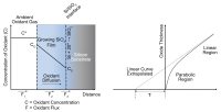
Chemical Vapor Deposition Physics
Chemical vapor deposition processes can be defined as: any process in which a thin solid film is formed on a substrate by the surface-mediated reaction of adsorbed precursors from the …
Technical Notes
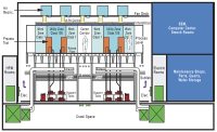
Semiconductor Fab Utilities Overview
Semiconductor fabrication utilities include ultrapure water, bulk high purity gases such as nitrogen and argon, exhaust gas handling and disposal, and cleanroom air systems.
Technical Notes
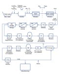
Ultrapure Water for Semiconductor Manufacturing
This technical note provides a basic familiarity with the design elements and functionalities for UPW systems. We will discuss the main UPW parameters, the treatment sequence for UPW …
Technical Notes
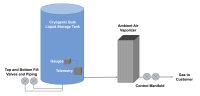
Semiconductor Gas Storage and Delivery
A variety of gases are employed for different purposes within a semiconductor device fabrication plant. These gases range from the pyrophoric and/or toxic specialty gases required for …

Technical Notes
Semiconductor Exhaust Gas Treatment
The process exhaust downstream from the cleaning, deposition and metal etch processes often experiences problems due to fouling often caused by the condensation and build-up of process …
Technical Notes
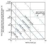
Cleanroom Ultra-clean Air Delivery
Semiconductor fab environments require ultra-clean conditions to ensure low numbers of product defects due to particulate contamination. A critical aspect in creating an ultra-clean …

Technical Notes
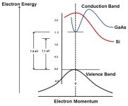
Electrical Conduction in Solids
The physical mechanism of electrical conduction in solids is best understood using a model that physicists refer to as "band theory", which is based on the idea that the state of an …
Technical Notes
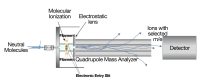
Residual Gas Analysis
Modern RGAs utilize quadrupole mass spectrometry as their underlying operational principle. Quadrupole mass spectrometers can monitor multiple gas-phase species in real-time with a …
 Ultra-High Velocity